
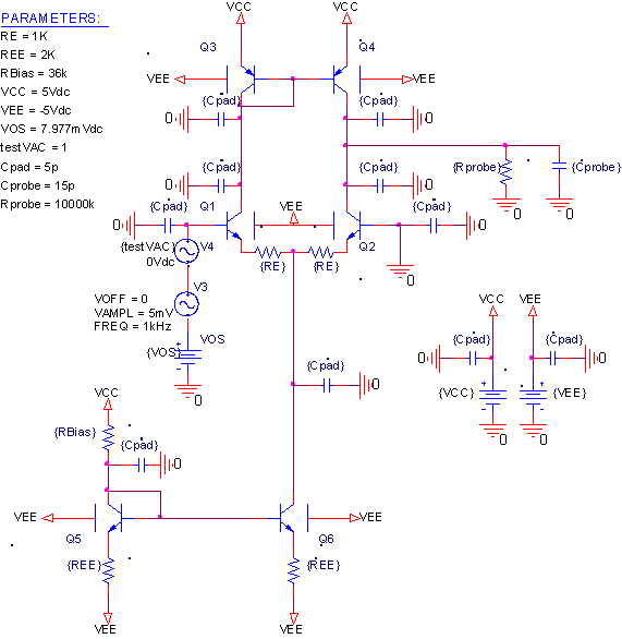
 Active-loaded differential amplifier. This is the first Stage of the op amp, with a 5o dB Gain.
 Class-AB output stage. This second stage alows for driving small loads and increases the overall gain a bit (~10 V/V).
Note: all circuit schematics account for the pin capacitance of the packaged IC (Cpad = 5 pF). Also the loading effect of the oscilloscope probe used to perform the experimental measurements is accounted for in the schematics by modeling the probe as a resistor (Rprobe = 1 MΩ) in parallel with a capacitor (Cprobe = 15 pF).
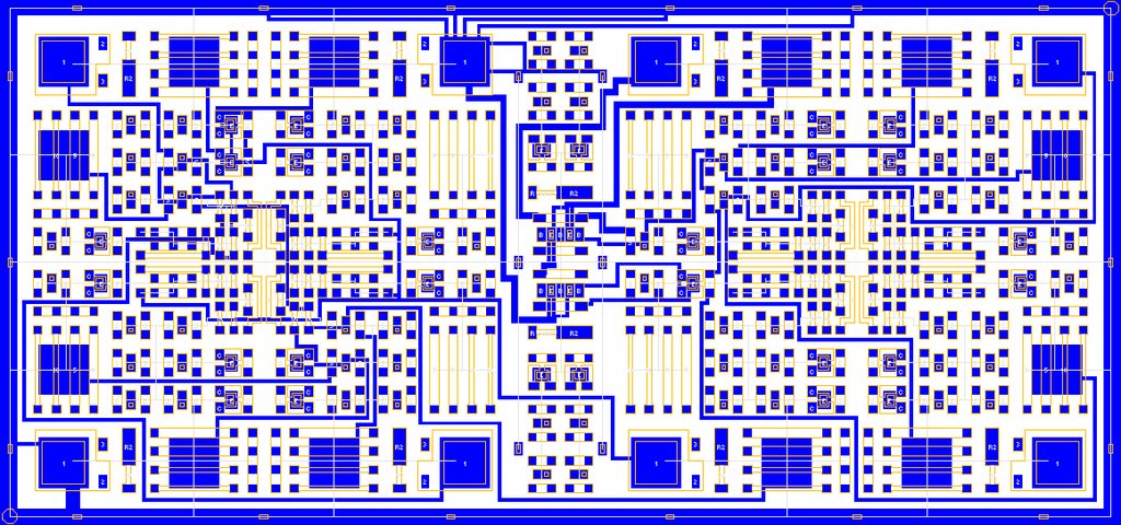 IC layout (done using Electric).
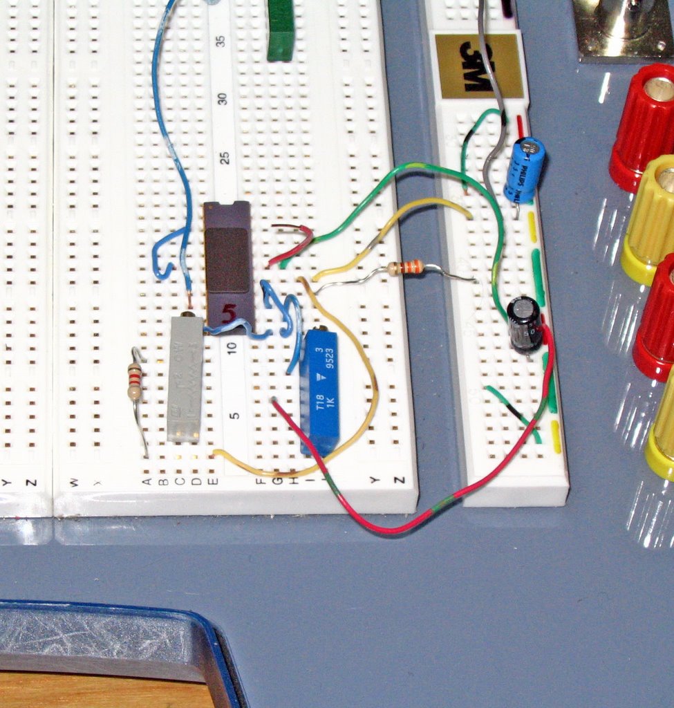 The chip (a.k.a. #5) being tested.
The chip in its natural environment.

A close up on the naked chip. Pretty neat.
I'll post more details soon.


1 comment:
what is an op amp?
Post a Comment